概述
计组课程的第二个大实验–实现多周期CPU。相比起单周期,多周期的特点是:一条指令的执行需要多个时钟周期。也就是说,不是所有指令都需要完全执行五个阶段,绝大多数指令只需要执行其中的3-4个阶段就可以了,多周期CPU就是基于这种思想实现的。要看代码的直接看https://github.com/leungyukshing/-CPU-
分析
大家之前都完成了单周期CPU,对于CPU的工作原理和Verilog的模块化编程都有一定的了解,这里就不再赘述。我就直接分析一下多周期CPU的工作特点。一条指令需要多个时钟周期,就要用到状态机,用于控制一条指令中不同的状态,这个状态机是存在于控制单元里面的。
然后是一些数据的寄存器,用于保存数据。多周期CPU可能会导致数据冲突,我们必须提供一个部件存储数据的一个状态。
代码实现
1.控制单元(ControlUnti.v)
控制单元包含了状态机、设置下一个状态、设置信号三个重要部分。我们需要根据当前指令设置下一个状态,根据当前状态设置控制信号。这与单周期CPU是类似的,同样是需要先构建一个控制信号真值表。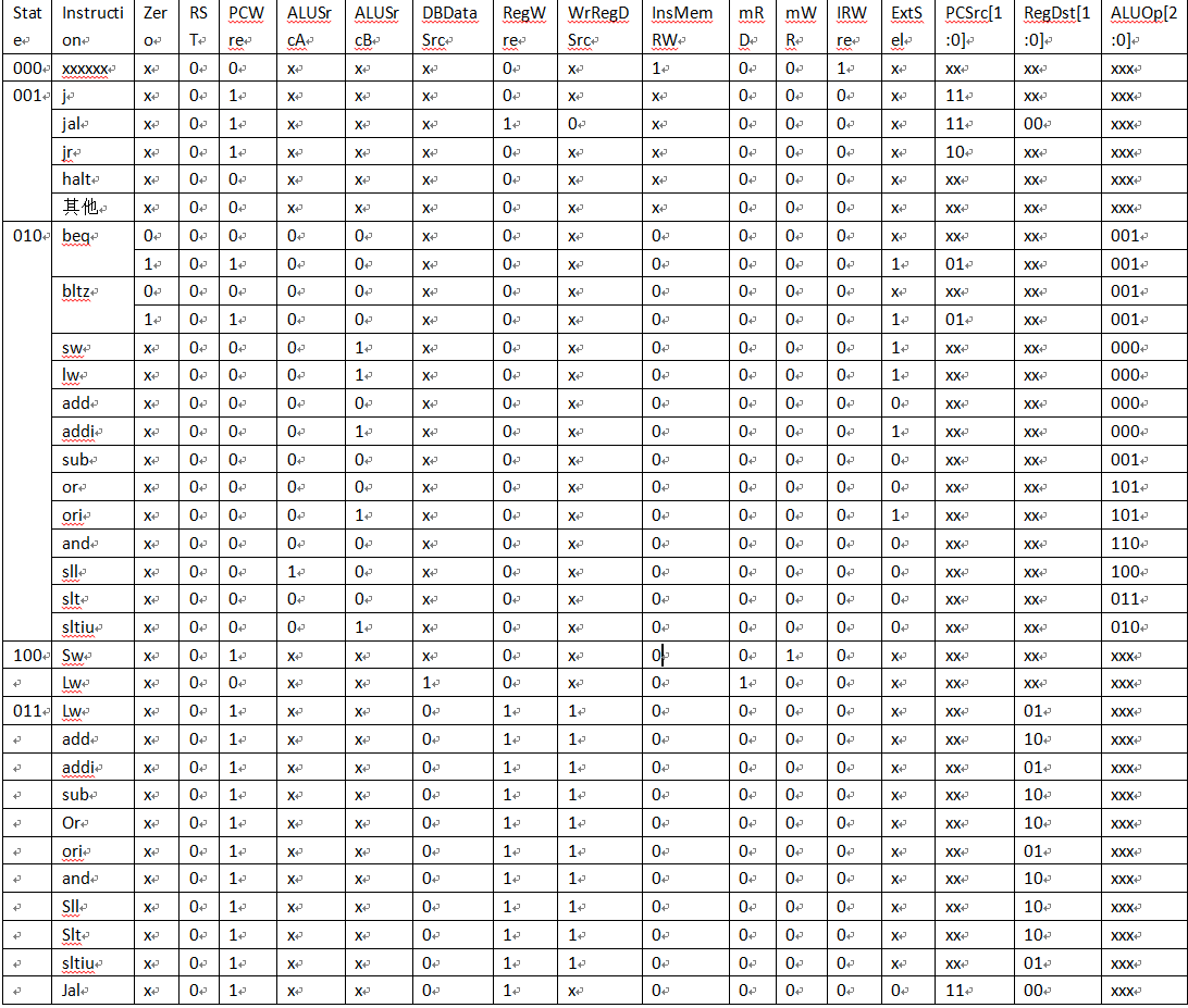
1 | module ControlUnit( |
2.程序计数器(PC.v)
PC的设置是使用时钟触发的,我是用的是上升沿触发。
1 | module PC( |
3.PC跳转地址合成(PCAdd.v)
对于跳转命令,指令中会有跳转的地址(一般是26位),我们需要合成一个32位的地址给PC。
1 | module PCAdd( |
4.指令寄存器(InsMEM.v)
这里我使用了一种与单周期CPU不一样的方式初始化寄存器。我们可以首先编写好指令代码在一个txt文件中,在初始化的时候就将内容读入寄存器中。
测试指令: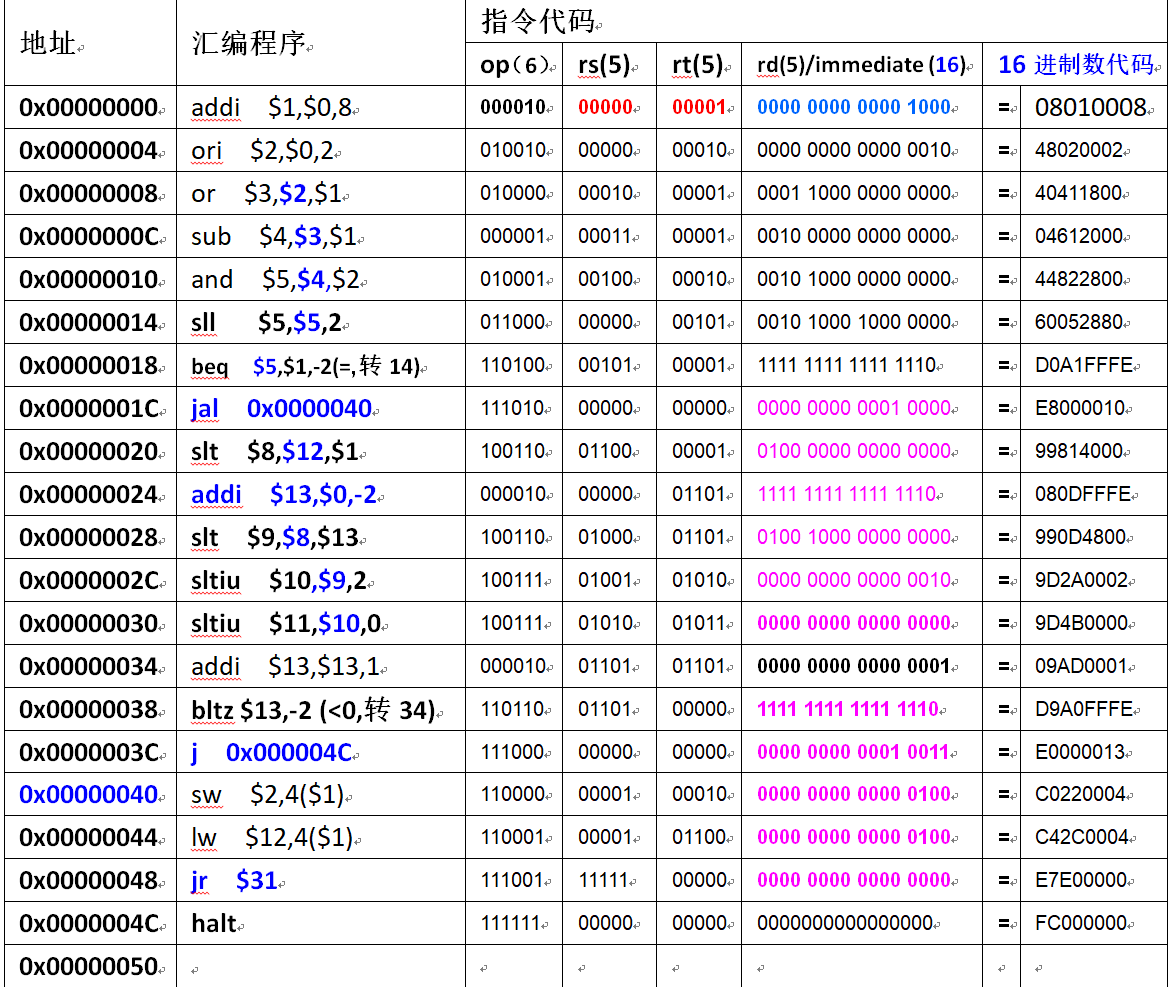
ins.txt文件内容: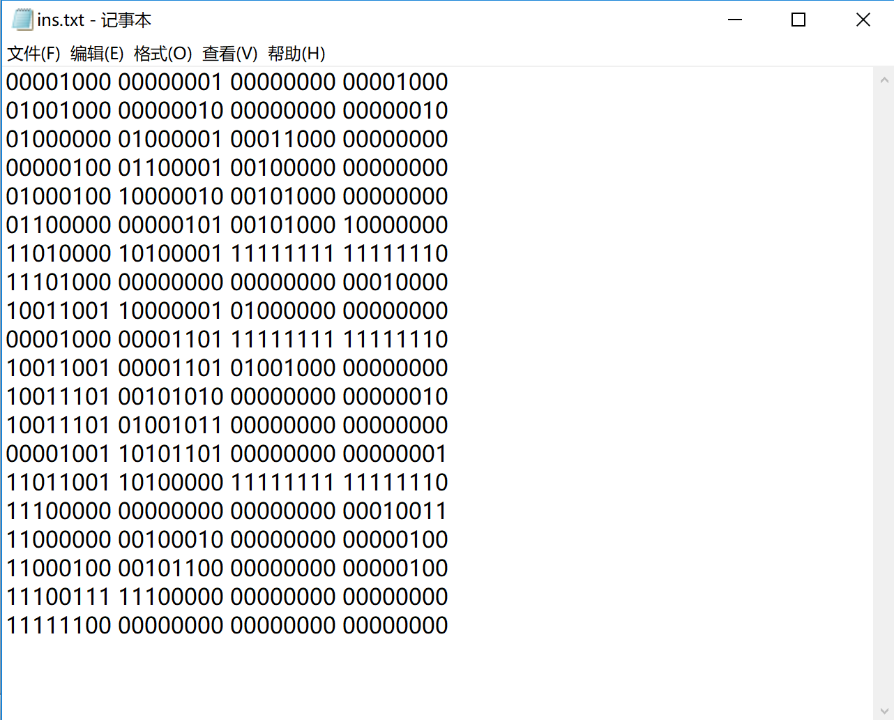
1 | module InsMEM( |
5.数据存储器(DataMEM.v)
由于控制读写的信号与状态有关,因此数据存储器的读写就不需要使用时钟触发了。
1 | module DataMEM( |
6.寄存器组(RegisterFile.v)
寄存器组的读写与单周期CPU类似,特别需要注意的是对于目标寄存器需要有一个数据选择器。
1 | module RegisterFile( |
7.算术逻辑运算单元(ALU.v)
这一部分和单周期CPU一样,不再赘述。
1 | module ALU( |
8.符号位拓展模块(Extend.v)
这一部分与单周期CPU完全一致。
1 | module Extend( |
9.二选一选择器(Selector_2_to_1.v)
整个CPU中有多个地方用到了数据选择器,因此我把它单独分离出来。
1 | module Selector_2_to_1( |
10.数据寄存器(DataRegister.v)
数据寄存器就是将数据保存一个时钟脉冲,用于解决数据冲突问题。
1 | module DataRegister( |
11.顶层模块(m_cpu.v)
连接上述各个模块,成为一个多周期CPU。
1 | module m_cpu( |
仿真测试与烧板
仿真测试
以上就是多周期CPU的主要模块,编写测试文件对其进行仿真测试。
测试文件(test.v):
1 | module test; |
部分测试结果: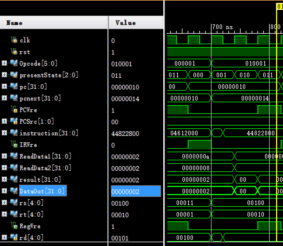
烧板
烧板的过程和步骤与单周期CPU基本一致,因此这里就不再赘述,详情可以参考GitHub里面的代码或者是参考单周期烧板介绍。
小结
多周期CPU的难点在于对指令状态转移的理解与实现,其他部分与单周期CPU类似,过程中还是会遇到很多问题,需要大家给多点耐心去看波形调试,烧板的部分下一篇post再分享,谢谢大家支持!

